Aura Semiconductors
1.Realize 10kΩ Resistor using unit Resistance of 3kΩ using any number of Series/ Parallel Resistors?
2.Realize 1.5pF Capacitor using unit Capacitance of 1pF using any number of Series/ Parallel Capacitor?
3)
4)

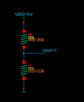
6
7. Conversion of Micro to Milli- 1uv= mV
8. Conversion of Milli to Micro - 1.25mv= uV
9. Conversion of Pico farad to Femto Farad- 0.2pF= fF
Given Sheet Resistance = 10Ω/square, W= 15um, L=1.5um, t=10nm

11. Draw Cross-Section of NMOS
Interview Questions
1. What is MOS?? Why do we use Poly instead of Metal?
2. Why the body is highly Doped ?? ( For example in NMOS we use P+ why can’t we use only P- or just P type)
3. If there is no Variation in VDD or GROUND Is there is a chance for Latch Up?
4. What care do you take to Prevent Latch-Up?
5. What is the Concept of Double Guard Ring? What is Deep-Nwell? How do you use it? Draw Cross-Section of it.
6. What kind of Shielding have you used in Layout?
7. Explain Working of Current Mirror? Why Current need to be Constant?
8. What is Coaxial Shielding? How did you do in the Layout?
9. What happens when P-Type & N-Type are in Contact?
10. What does atom consist of?
11. What do you conclude from Violation of Electro migration? Why there is a violation? What happens if it exceeds EM Limit?
12. Explain EMIR analysis using R3D
13. What is DRC? Why DRC?
14. What is LVS? How does Tool Understand?
15. What is ERC? What is Stamping Error & Soft Connections?
16. What is DFM? Which is better DRC/DFM? Why do we go for DFM?
17. What is Density? Why do we need to do Density check? What happens if we don’t do it.
18. Explain about Parasitic? How it is formed? Which Tool did you use?
19. What difference have you observed when you worked from 180nm to 65nm? Which Technology node had more Capacitance and why?
20. What is Antenna Effect? Why there is Breakdown of Gate Oxide?
21.What is HVDRC? Why do we need to have it? Why more spacing for HVDRC?
22. For A=2 (Current Mirror), B=3, C=3, D=4 How do you Match?
23. What is the advantages of Half-Cell Technique?
24. What is the Advantages of Using more number of Segments of Resistor/ Capacitor in Layout?
25. If there is a sensitive signal how do you protect it without shielding?
26. When Schematic is given how do you start it?
27. Explain Block Diagram of BGR?
28. Vertical Cross-Section of BJT?
29. Considerations taken to do BGR Layout?
30. Draw Schematic of Error Amplifier?
31. How do you do Routing of Clock-Tree?
32. Identify Capacitance between Metal to Metal & Metal to Substrate? Also find Fringe Capacitance?
33. What is STI? Does Shared devices have more STI or unshared device have more STI?
34. How do you Minimize Capacitance in Layout?
35. Why do we need to Follow Metal Orientation?
36. Necessity of Matching while doing Floorplan?
37. Requirements of Dummy in Layout?
38. Cross-Section of Poly Resistor?
39. What is the Application of Using more Number of Resistor? Where is it used?
40.
41. Two Cap having different width will they have different Cap?
42. Explain Isolated nmos?
43.

Is it Matched?
A B A B
44. How do you match if A=5, B=5?
Comments
Post a Comment