Posts

Showing posts from July, 2021

Tessolve Semiconductors -Fresher (Validation Engineer)

Image
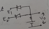
1.       Round 1       1. Problems on Equivalent Resistance 2 Operation of CMOS Inverter 3. Problems on Transient, Steady state Analysis 4. Problems on calculating Equivalent Resistance in Op-Amp circuits 5. What is loading effect? 6. Operation of Inverter with R in place of pmos & NMOS , disadvantage in connecting in that way? 7. Latch and Flip-flop difference 8. What is test Engineer Job Role. 9. Problems on Expected Clock period to overcome Setup violation 10. Ideal characteristics of Op-Amp.   ROUND 2(45min) 1.  W hat it diode, operation of diode   2. what is transistor, what happens if voltage is increased ?   3. Avalanche Breakdown 4. Applications of diode 5. Identify Essential Prime Implicants (EPI), Prime Implicants in given problems 7. Can Flip flop be built with Latch ?   8. Can Latch be built with clock? 9. What is kelvin Connection ? 10. Uses of Buffer ? 11. Draw Inverting, non-Inverting Integrator, Differentiator using op-amp & output Voltage formulas for t

AMD Interview questions - Physical Design

(1st round -- 45 minutes)**  1) Introduce myself.  2) Operation of MOSFET.  3)Types of MOSFET.  4) What is the difference between BJT, MOSFET and CMOS.  5) Why CMOS. 6) Why cmos for low power applications.  7) Basics questions on current equation of MOSFET.  8) basic questions on layers of MOSFET.  9) What is threshold voltage.  10) some questions on equation of threshold voltage.  11) PVT parameters.  12) what is the secondary effects.  13) Voltage divider rule.  14) series circuit operation.  15) parallel circuit operation.  16) oscillator operation.  17) universal gates.  18) Realization of XOR and XNOR using NAND and NOR gates.  19) Which has highest area NAND or NOR and Why.  \20) ASIC vs SOC. (2nd round --- 45 minutes )*   1) Introduce myself.  2) Complete PD flow.  3) inputs to the PD tool.  4) Some commands on Innovus tool.  5) what are the end cap cells why its used in placement.  6) what is congestion.  7) Disadvantages of Congestion.  8) How do you transfer clock signal from

PCB Layout Questions

Q1: 1. PCB design flow explain? Design Flow Process 1. DESIGN REVIEW 2. COMPONENT DATA SHEETS 3. MECHANICAL DATA IMPLEMENT 4. LIBRARY MANAGEMENT 5. CONTRAINT SETTING 6. PART PLACEMENT 7. POWER & SPLIT PLANES 8. ROUTING CRITICAL NET 9. SIGNAL INTEGRITY 10. ROUTE REMAINDER OF NON-CRITICAL ROUTES 11. FINAL DRC CHECKS  12. SILKSCREEN & ASSEMBLY 13. FAB LAYER UPDATION 14. FINAL CAM OUTPUT Q2 : What is EMI/EMC? where does these exits & how to control them? Answers: EMI: It is the process which gives out disruptive EM waves, transmits energy from one electronic device to another via radiated/conducted paths. In common usage, the term refers to RF signals. EMC: The capability of electrical/electronic systems/equipment & devices to operate in their intended EM environment within a defined margin of safety & at design levels/performance, without suffering or causing unacceptable degradation as a result of EMI. Where does exits: Any source of changing voltage anywhere in the c

Texas Instruments- Analog Layout (3+ Experience)

  Interview Questions   1. What was the total number of pins in Layout of Top level?   2. Did you manually connect pin/ tool?      Virtuoso-L (We need to connect manually the pins)      Virtuoso XL- Generate from Source (All pins will be dumped but need to do the Connection)   3. Who was the Team lead?   4. Did you do Floor plan from scratch or already Floor plan was done?   5. How did you clear antenna error? Did you get antenna error in layout?   6. Was there any two separate grounds in Layout? How did you run LVS?       Using Tub (Use NRING to separate between two grounds one is the black screen)   7. Did you handle Digital part?

Micron Serdes Interview (3+ Experience)

  Interview Questions 1. Blocks done in 65nm SERDES (Custom Digital, hyst_buf, Voltage Regulator) 2. Challenges faced in the Blocks of SERDES      3. What was the Current (Electro Migration) 4. Which was the tool used to run Electro Migration 5. Are you aware of Latch Up issue? Did you get any DRC for Latch Up? 6. Explain Floor Plan with Schematic and Layout

Cadence Analog Layout (3+ Experience)

  Interview Questions 1. Tell me about yourself? 2. Draw the Block Diagram/Circuit of LDO?          3. What is Diode Connected/ Current Mirror? 4. Consideration of Floor Plan?   5. Drawback of Common Centroid Matching? Ø   Two rows. Ø   For lower technologies it can be harmful for the gates and generally not used. (channel length is less) Ø   Larger set of gates is the routing that is required to connect them. (This could add capacitance) Ø   Complex routing, more CAP, more area   7. How to minimize parasitic? What happens if Parasitic is present? Ø   Time increases, Delay Increases Ø   Keeping apart, Going for Higher Metals, Overlap Drain/Source, increase the spacing of all the nets from the net which is critical Ø   Use higher metals for the net in which parasitic capacitance is important. Ø   Increase the spacing of all the nets from the net which is critical (for which parasitic capacitance is important). Ø   Put some other reference signal (with w